RFID Lab
In this lab, we explored the workings of an RFID card access system. We were able to read the information off the card, paving the way for future work in mimicking the ID card to the reader.
Previous Work Link to heading
We took inspiration and information from work done by previous groups:
- The MIT ID Card System: Analysis and Recommendations
- RFID Tunnel Project Report
- Arphid - anonymous post
Background Link to heading
RFID forms the backbone of access control systems in many different areas. In particular, an ID card contains a passive RFID transmitter that can be tapped against a card reader to unlock certain doors. There are many different variations on RFID, but the one we examined uses a low-frequency, passive system (supplied by Indala system from HID Global).
RFID Basics Link to heading
Without going too much into detail, RFID refers to technology that uses radio waves to track tags on objects. It does this by encoding information in the radio waves that a reader then picks up. There are many different variations on the basic RFID system. The one that is most relevant to the ID card (and most tap-access ID door systems) is called passive RFID. In a passive system, the tag (in our case, the ID card) does not have a source of power. Instead, the circuitry on the card is actually powered by the card reader. The card reader broadcasts a signal and the coil on the ID card acts as the secondary winding on a transformer, transferring power to the card.
Detecting Phase-Shifted Signals Link to heading
The actual method of sending data across the signal is known as phase-shift keying (PSK). Bits are sent using the wave by creating phase-shifts to signal bit flips. Before getting into how the data is encoded, we first need to understand the concept of the 125 kHz wave as a carrier wave. The data is actually encoded on half the frequency of the carrier (i.e. at 62.5 kHz). This signal is carried by the 125 kHz wave that is sent back to the reader.
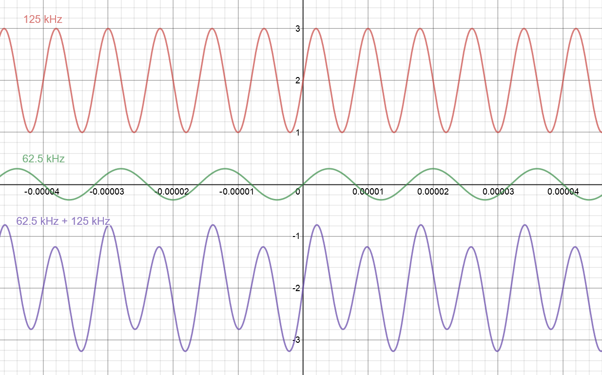
Figure 1: Base carrier frequency from the card reader (red), 62.5 kHz signal that encodes the information (green), the resulting signal sent back to the card reader as the sum of the carrier and the data frequency (purple).
Notice in Figure 1 how the resulting purple waveform is actually the sum of the carrier frequency and the data frequency. Because the data frequency is half the carrier frequency, the carrier frequency has alternating high and low peaks. The actual data frequency is visible in the envelope of the carrier frequency. One more important concept for phase-shift encoding is the phase-shift itself. In our system, we use a form of PSK known as binary PSK (BPSK). In this protocol, we use 180-degree phase shifts to convey information. Coincidentally, a 180-degree phase shift corresponds to simply inverting the signal vertically. Figure 2 shows two different methods of phase shifting.
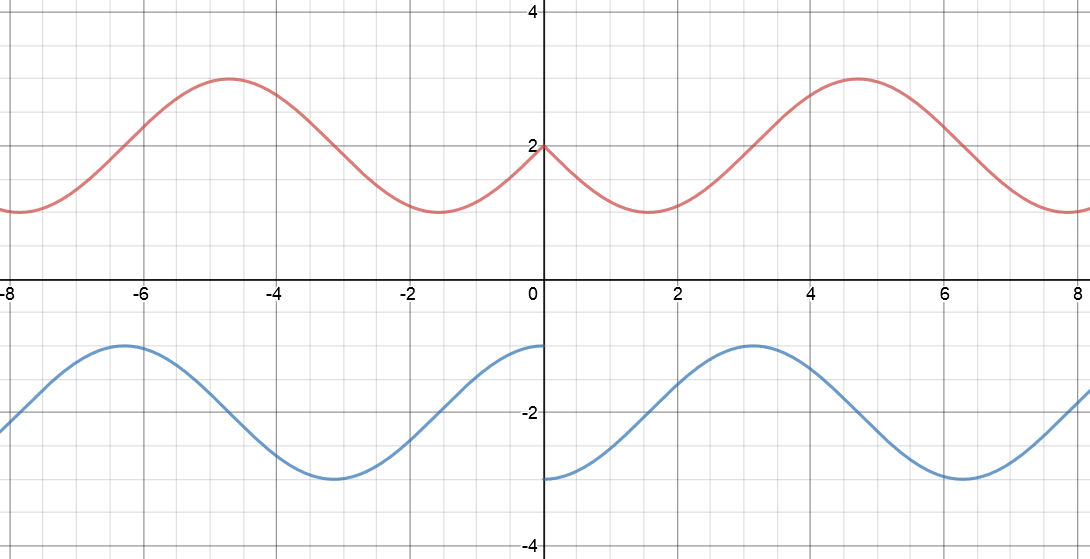
Figure 2: The red waveform shows the phase shift occurring at the zero crossing. The blue waveform shows the phase shift occurring at the peak of the wave.
The red waveform in Figure 2 shows what’s called zero-crossing BPSK. The phase shift occurs when the waveform crosses zero. This scheme is generally preferable because the sharp edge transition in the blue waveform potentially introduces noise into the system.
Now, we are ready to see the effect of the phase shift on the carrier signal. Figure 3 is Figure 1 repeated except with a phase shift in the signal that carries the data.
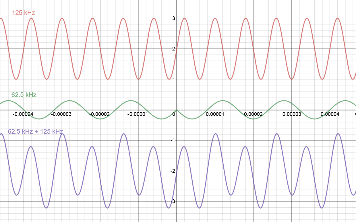
Figure 3: The effect of a phase shift on the carrier wave. The purple wave has two consecutive low peaks due to the phase shifting.
Notice in the normal modulated carrier wave, the 62.5 kHz modulation causes alternating high and low peaks in the carrier. The effect of the phase shift is to cause two consecutive high points or two consecutive low points. This is a very distinctive characteristic that we can take advantage of to detect a phase shift. Note that we are using a more unconventional way of detecting this signal. More traditional demodulation approaches involve multiplying the signal with the original carrier wave to recover the data. However, for our purposes, the use of a comparator is sufficient.
We use a comparator set at the right level to detect the peaks in the signal that is broadcast by the card. Notice in Figure 4 how the falling edges on the comparator waveform are much farther apart when there is a phase shift. This can be detected by a microcontroller which can now decode this signal.
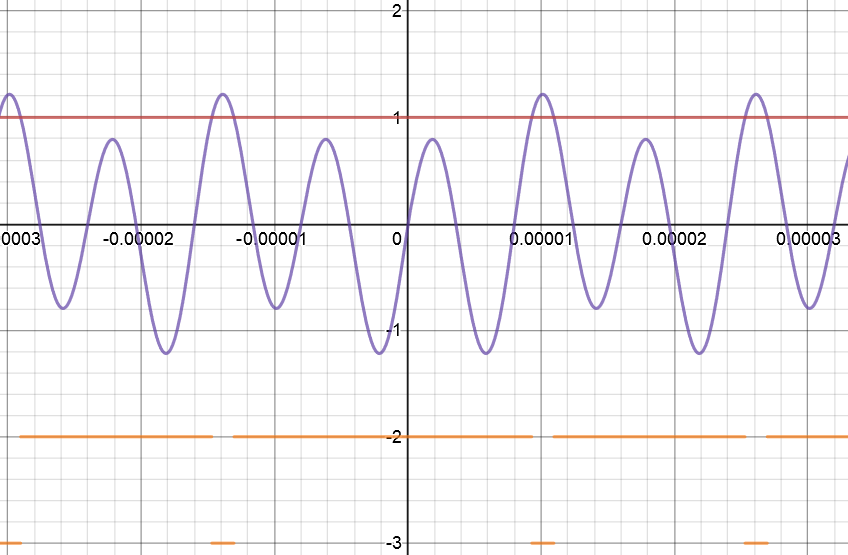
Figure 4: A comparator can be used to detect when the modulated signal (purple) goes above a threshold (red). The comparator output is shown in orange.
As a side note, the details regarding how the RFID tag actually generates this signal and modulates the carrier wave is beyond the scope of this particular project. I will most likely do another writeup going through the details of that and showing how to use a microcontroller to spoof the card itself. For now, we will concern ourselves with just reading the card.
Data Encoding: Phase Shift Keying Link to heading
The last question that remains about this system is how the data is actually encoded. That is, how do we use the idea of phase shifting to actually convey an ID number? The protocol used by our ID system sends one bit every 16 cycles of the data signal (i.e. the 62.5 kHz wave). If the next bit is different from the current bit (i.e. there is a bit flip), then the tag will phase shift the data signal by 180 degrees. Otherwise, the next bit will be assumed to be the same as the previous bit. Because this protocol relies on knowing the previous bit, we need to know what the first bit is. The protocol also specifies that the data packet will always begin with a long string of 0s. This gives us the initialization value. 1
Circuit Link to heading
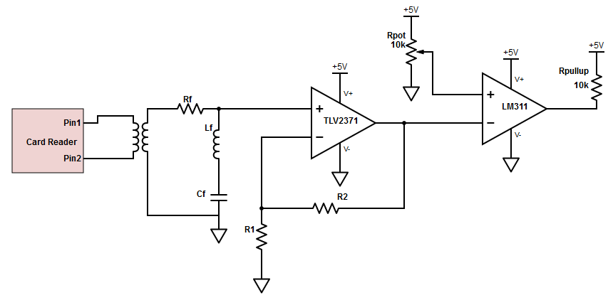
Figure 5: Full circuit for reading the data off an ID card.
The card reader on the far left is modeled as the primary of an air-core transformer. The RFID card contains a pickup coil which is modeled as the secondary of the transformer. When testing this in lab, we used a signal generated hooked up directly to a 3-inch diameter coil of wire with about 10 turns on it to simulate the signal the card reader is producing.
The first stage of the circuit cleans up the signal. The desired information is contained within the 62.5 kHz wave; however, this is still superimposed on a strong 125 kHz signal. To remove this, we found that a notch filter works well for this purpose. Lf, Cf, and Rf formed the notch filter.
Afterwards, the signal needs to be amplified. This was done with a TLV2371 op-amp. To avoid loading down pickup coil and the notch filter, a non-inverting amplifier configuration was used.2 We found a gain of 20 to be sufficient.
In the final stage of the circuit, we actually decode the signal. The LM311 is an open-collector device so the pullup resistor is needed to pull the output high.3 This was necessary during testing, but when it was connected to the Teensy, we just configured the internal pullup resistor to perform this function. The output of the LM311 goes into the Teensy.
Code Link to heading
The resulting comparator output was read by a digital pin on a Teensy 3.1 which was the microcontroller used by the class for all the labs. A falling-edge-triggered interrupt was used to detect edges which would then be processed by the main work loop. The edge interrupt calls an attached interrupt service routine (ISR). It is good practice to keep the ISR as short as possible, so the ISR simply records the elapsed time and raises a boolean edgeFound flag which is then polled by the main work loop.
The most straightforward way of approaching the code for the work loop was by implementing a state machine. There are four states for the microcontroller: WAITING, TRIGGERED, CONSTANT, and PERSONAL. The first two states handle initialization and reading the initial sequence of zeros while the last two states handle reading the constant bits and the personal bits respectively. The work loop polls the edgeFound flag, and when it finds and edge, runs through the state machine logic.
- WAITING: The microcontroller defaults to the WAITING state. In this state, it simply waits until it finds 30 consecutive zeros. There is some additional logic to perform the correct initializations for next stage. Once 30 zeros are found, the state transitions to TRIGGERED.
- TRIGGERED: this state simply waits for a phase shift (i.e. a bit flip) before transitioning to the CONSTANT state. This assumes that the constant starts with a 1 and helps prevent frame-shift errors which might occur if the previous data packet ended with a string of zeros.
- CONSTANT: in this state we start reading the constant bits until we have enough bits to transition into the PERSONAL state.
- PERSONAL: this state accumulates the personal bits. Once enough bits have been found, it first checks the constant bits to determine if the card is indeed for the MIT system and then looks through the database of pre-recorded personal bits and attempts to look up the name associated with the card.
The biggest challenge faced when writing this code is correcting many off-by-one errors during the reading of the different bits. While the Teensy is running at 96 MHz, the pulses are occuring at a frequency of 62.5 kHz, so print statements need to be used cautiously to ensure that they do not interfere with the timing.
Further Work Link to heading
The other half of this project involves implementing an RFID spoofer. While there currently exist purpose-built, monolithic IC solutions for modulating the incoming 125 kHz signal, it is elucidating to implement a system that can also perform this modulation, for example, through a Teensy. One benefit of this is that if a brute-force attack is being attempted, it is much faster to simply have a microcontroller run through the different sequences rather than have to re-program an IC for each attempt.
Footnotes Link to heading
In practice, this string of zeros most likely serves as a synchronization sequence for the decoder in commercial RFID readers. The string of zeros creates a long sine wave that is uninterrupted by phase shifts. This allows something like a phase-locked loop to synchronize the reader’s clock with the data signal since the decoding process requires multiplying the modulated signal by the unmodulated version. ↩︎
The non-inverting amplifier configuration sends the signal directly into the non-inverting input of the op-amp. Becuase the input impedance of the op-amp is high, this prevents current from flowing out of the circuit and into the amplifier. In other words, from the point of view of the notch filter, the op-amp does not exist. This is opposed to an inverting configuration in which the signal travels through two resistors which will present a much lower impedance than that of the op-amp. ↩︎